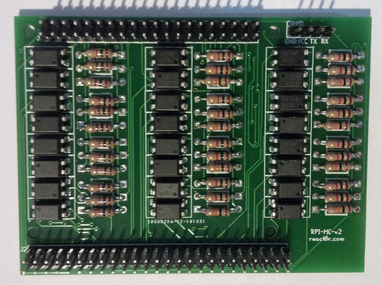
This project used:
- Terrabloom 6" fan (ECMF-150)
- Raspberry Pi 3 (or Zero W)
- 2x BC547 transistors
- 2x 1k Ohm and 2x 22k Ohm resistors
- Single sided copper FR1 copper plates
- Genmitsu 3018 Pro CNC
- Genmitsu leveling probe
While grinding on other projects, sometimes you need a change of pace and I had a cooling fan I wanted to automate so here we go. The Terrabloom ECMF-150 fan can easily be controlled via pulse width modulation (PWM) from a Raspberry Pi and has resources on how to set it up. To control the fan, the manufacturer recommended using a logic level shifter. After looking at the circuit, I became excited to see what the state of low-cost PCB milling machines using free and open source software (FOSS) would look like. Then, I decided to turn it into a blog for my own documentation. Hopefully you find it useful or at least entertaining.
Circuit Background
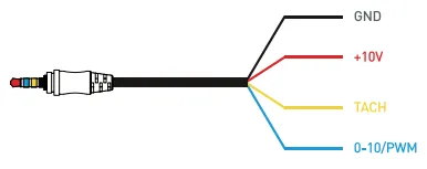
First, some background on why the level shifter is needed. The RPi GPIO pins output at 3.3V while the Terrabloom fan uses 10V for its control. This means the 3.3V needs to be shifted from 3.3V to 10V. Fortunately, the pinouts on the control line include a 10V power supply.
Initially, I was going to use gEDA to create the schematic for the circuit as I was already familiar, but turns out it’s no longer being maintained and so is no longer available in my Linux distribution of choice. However, the popular FOSS package KiCad is. Watching a few tutorials on how to use it got me caught up to speed. It was very similar to other electronics design software so it was easy to pick up. Here is the schematic produced for reference:
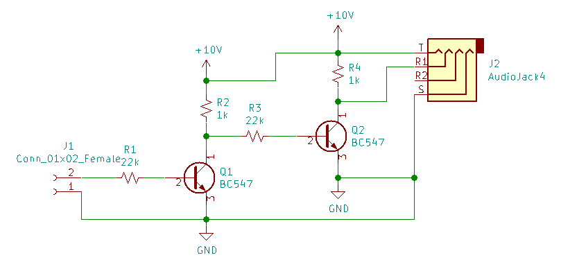
In the schematic, two BC547 transistors are used to shift and then invert the signal sent from the Pi. The 3.3V GPIO line (left) is used to control the gate of the first transistor Q1. Note, this sets the output on the line into R3 as 10V when the gate (or GPIO) is OFF. This behaviour is inverted to the specifications given in the fan manual. A 10V signal in will turn the fan on. Thus, a second transistor (Q2) is used to invert the signal from Q1 to produce the expected behaviour. Of course, the inversion could have been handled by software on the Pi but I decided to go with the recommended circuit to favor expected behaviour. Also notice the resistors are 22k Ohms instead of the recommended 20k Ohms from their video. I didn’t expect this to be outside tolerances and a test on a breadboard confirmed this. The only reason for this decision was that 22k resistors were on hand.
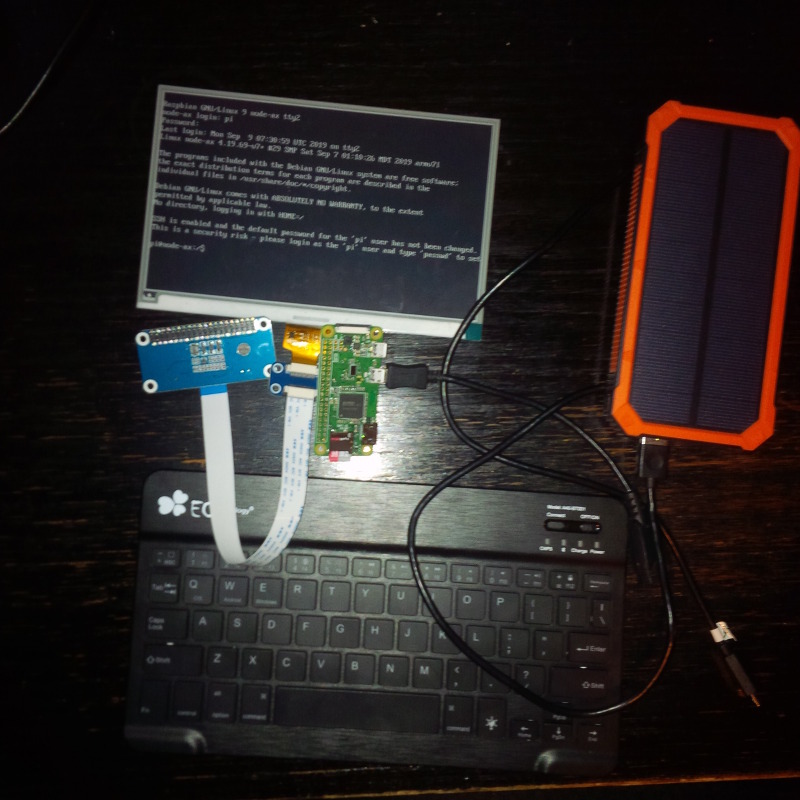
With the above circuit, I can control the fan with Python GPIO libraries on the Pi. To test it all to make sure it worked, including the 22k Ohm resistor choice, I soldered a jumper on to a Raspberry Pi Zero W and tested the circuit with a breadboard.
Testing with a Raspberry Pi Zero W
If you’re only interested in PCB milling, you can skip this section.
Raspberry Pi Zero Ws have two micro USB ports. One port is to supply power to the board and the second is for USB data or power. Most blogs have you connect up a keyboard and monitor to get it set up, but I found that to be such a headache, lugging around monitors and such. Given my work in the mobile and embedded world, I wondered if there was a better way.
Turns out there is. The data USB port can configured as a USB/ethernet gadget or device instead of a USB host. The RPi being a single board computer (SMB), one would expect the USB port to be configure as a USB host. However, with a Linux kernel device overlay and a boot command line option, the USB port can be configured as a device. That is, you can plug the Zero W into another computer and connect to it over a private network created over the USB port.
To set up the Zero W, add the following to the boot partition:
- Add
dtoverlay=dwc2toconfig.txt - Add
modules-load=dwc2,g_ethertocmdline.txtbeforequiet - Create the file
sshto enable SSH on boot:touch ssh - Re-add default user (on first boot):
echo "pi:$6$egCQhAWc4oE/k4y5$suXvtT77o1/2V.4BFcgvICSsFgX6kdW9Cap3zpjq9GKtgiHKZqGIlMaFbeotKyeFHtVDLhfou7MTgsmB7c7D51" > userconf
The last step is required for the newer Raspbian OS images. As of bullseye, the default pi user has been removed. To recreate it on first boot, the last step is needed. See this post for more information. Though I had troubles with it and had to manually correct it in the shadow file.
After set up, everything worked pretty much as expected. The Linux system I was plugging the RPi into recognized the device and initialized the ethernet device. Unfortunately for me, NetworkManager on Debian kept trying to get an IP via DHCP. This was causing the interface to come up and down as DHCP was failing on that private network. The intended behavior by the Raspbian OS developers was to have the device assign a link-local IP address and use mDNS, then have users connect via ssh [email protected]. For those unfamiliar with mDNS, multicast (not broadcast) packets are sent over the local link, advertising itself and asking for DNS resolution. This resolution only really applies to the .local namespace.
To get NetworkManager to manage the private interface properly, the following setting modification was required:
nmcli con modify 'Wired Connection 1' ipv4.method link-localBe sure to check and use your connection name instead of Wired Connection 1.
Also, if there are any other RPis on the network local to your PC, you can rename them by changing the host name that resolves to 127.0.1.1 in /etc/hosts to get the avahi daemon to use that hostname as its advertised host name.
I burned half a day on that but I think the research was useful. Setting up Zero W’s like that makes them way less cumbersome.
Once connected, the usual:
cd /sys/class/gpio
echo 23 > export
echo out > gpio23/direction
echo 1 > gpio23/value
Allowed me to test that a high 3.3V on the GPIO23 pin caused a 10V to show up on the R1 ring on the schematic. On to fabrication!
PCB Fabrication
To fabricate the circuit, a series of software packages are needed to take a KiCad-generated layout to something the CNC can use. Like many (most?) CNCs, the Genmitsu 3018 uses a GRBL firmware on the controller and this firmware uses a format called G-code to control the machine. On the KiCad side, like many (most?) electronics design packages, circuit layout can be exported as Gerber files. So I needed something that takes Gerber files and outputs G-code. Besides generating the G-code, I also needed software to send the newly generate G-code to the CNC machine over its control bus. As a side, this bus typically seems to be a standard serial device provided over USB.
The top two suggested open source packages for G-code generation in my search were FlatCAM and pcb2gcode. FlatCAM is written in Python and offers a GUI to visualize all the variables to generate the G-code from the Gerber files. I found the GUI largely unnecessary, as visualizations are already typically done by the command-sending software. The pcb2gcode tool is written in C++ and is only for the command line. So I chose pcb2gcode for it’s simplicity and user recommendations, and pressed on.
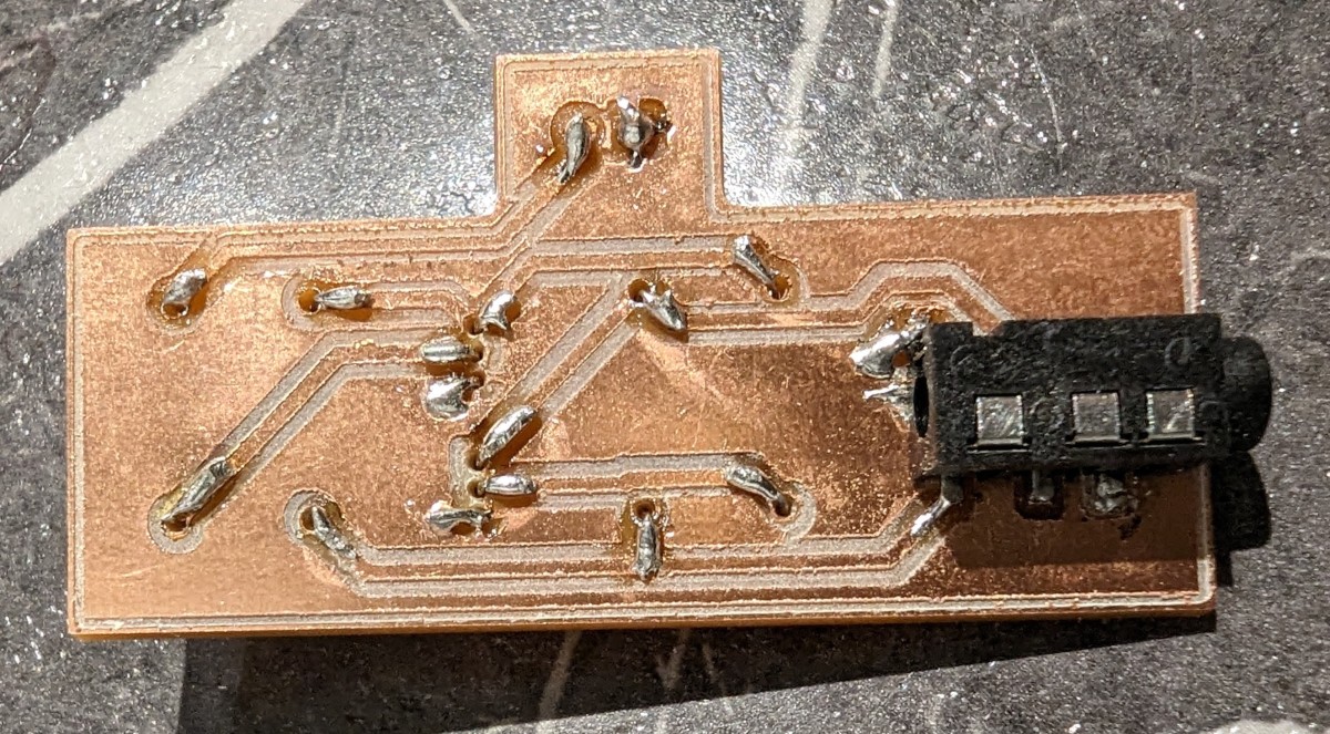
At this point knowing that there were several open source options to get the CNC to print the PCB, I started on the PCB layout. At first, not knowing the capabilities of the CNC machine I used the default design rules provided by KiCad. That is, 0.2mm clearance and 0.25mm track (aka trace) width. The former defines the space between elements where there should be no connections and the latter defines the width of connections or tracks between components. On my first print, I quickly discovered a 0.25mm track is way too thin, especially for someone trying to figure out what the machine is capable of.
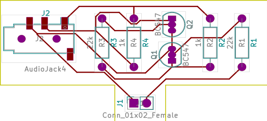
A few videos on YouTube demonstrated decent results with 1mm tracks, so I increased the width on all tracks and added a ground plane to make it easier to route. One mistake I made here is that the ‘Edit->Edit All Tracks and Vias’ tool along with adding the ground plane did not detect two tracks that connected to ground. If you use that tool, be sure that nothing gets unintentionally connected. I actually had the board printed and soldered before noticing two pins on a transistor were both connected to ground and I was very sad.
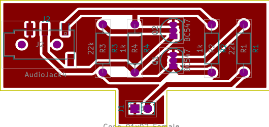
The resulting board was much easier to print and corrected grounded tracks.
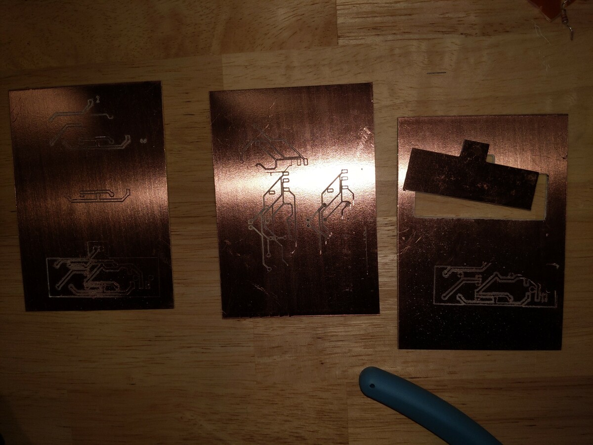
Of course, in between the two board designs there were quite a few tests and unsuccessful prints. Mostly while trying to configure software with desired parameters.
Below is the pcb2gcode millproject that stores gcode generation parameters. Parameter comments are given after.
front=terrabloom-logic-level-shifter-F_Cu.gtl
#back=board.back.gbr
outline=terrabloom-logic-level-shifter-Edge_Cuts.gm1
drill=terrabloom-logic-level-shifter.drl

# inputs in metric
metric=1
# gblr reports error
nog64=1
zchange=10

# parameters for isolation routing / engraving / etching
#voronoi=1                      # uncomment for voronoi regions
#offset=0.10            # uncomment for 20mil isolator
offset=0.1
zwork=-0.10
zsafe=1
mill-feed=200
mill-speed=12000

# parameters for cutting out boards
cutter-diameter=1.2
zcut=-2
cut-feed=100
cut-speed=12000
cut-infeed=0.7

# drilling parameters
zdrill=-2
milldrill=1        # Mill instead of drill holes
min-milldrill-hole-diameter=0.1
#zmilldrill=-2
drill-feed=25
drill-speed=12000
nog81=1            # Not valid for GRBL (3018)
nom6=1
Some comments about the parameters:
- front/outline/drill – Gerber files to read to convert into gcode.
- metric – All inputs in metric, usually millimeters.
- nog64 – Do not use the G64 code as it causes an error.
- zchange – Height when tool changes are needed.
- offset – How much in to offset from tracks, making them larger.
- zwork – Depth at which to cut into the PCB for making tracks. Here, zero is where the mill touches the board and -10 is 10mm into the board.
- zsafe – How high is it safe when moving the drill tip around. How high should the tip be raised when moving around during milling.
- mill-feed – How fast to move while milling in mm/minute.
- mill-speed – Spin speed of the drill while milling in mm/minute.
- cutter-diameter – Amount by half of which the tool path is outset from the shape in the outline file.
- zcut – How deep to cut when cutting out the board. The PCB is 1.6mm so 2mm should be enough.
- cut-feed – How fast to move while cutting in mm/minute.
- cut-speed – Spin speed of the drill while cutting in mm/minute.
- cut-infeed – Maximum cut depth before taking multiple passes.
- zdrill – Depth when drilling holes.
- milldrill – Enable mill drilling where holes are milled out to the desired size.
- min-milldrill-hole-diameter – The minimum diameter of the mill drill bit.
- drill-feed – How fast to move while drilling down in mm/minute.
- drill-speed – Spin speed of the drill while drilling in mm/minute.
- nog81 – Don’t use GRBL-incompatible one-pass drilling.
- nom6 – Don’t use GRBL-incompatible M6 tool change code.
For the command sender software, I initially chose Universal G-code Sender (UGS). It was close but found that it didn’t quite do the trick for PCB milling. This was largely due to the lack of functioning autoleveler. An autoleveler is used to create a height map of the surface using a probe. This is accomplished by attaching one lead to the copper PCB and one lead to the drill bit via alligator clips. As the drill bit is slowly lowered, the position is monitored and recorded the moment the circuit between the plate and the drill bit is closed. This is done for multiple points on the surface. It took a few guesses to find a good resolution at which to sample the PCB. I found 5mm seemed to be good enough for the layout that was roughly 55m by 25mm.
After a bunch of trial and error from setting up the software and CNC positioning properly, I was disappointed to see UGS throw an error when attempting to apply the height map correction data to the G-code. So I had to switch to bCNC. PCBs tend to have some bend in them, especially when they’re cheap and I found this makes it difficult to etch the thin layer of copper off. I only had a V-shaped milling bit which meant that if the surface was too high, the copper wouldn’t be removed. If too low, the V-shaped bit would take too much material off on the sides, leaving very thin tracks. So the functioning autoleveler in bCNC was crucial.
Two notes about the autoleveler:
-
When probing, the drill bit would move slow and stop immediately on contact. If the PCB wasn’t properly fastened to the plate, the autoleveler would record a higher position than needed. When milling, the bit would come down on the PCB and only slightly push it down. Without sufficient pressure, the bit would only score the surface instead of remove the copper. This could potentially be corrected with a deeper
zworkparameter in pcb2gcode but may cause deeper cuts on other parts of the board. -
In bCNC, doing an autolevel scan automatically applies the height map to commands as they’re sent. There is no need to apply the autolevel to the gcode with the Autolevel button. If you do, you need to clear the height map otherwise the correction gets applied twice.
My final print looked like this:
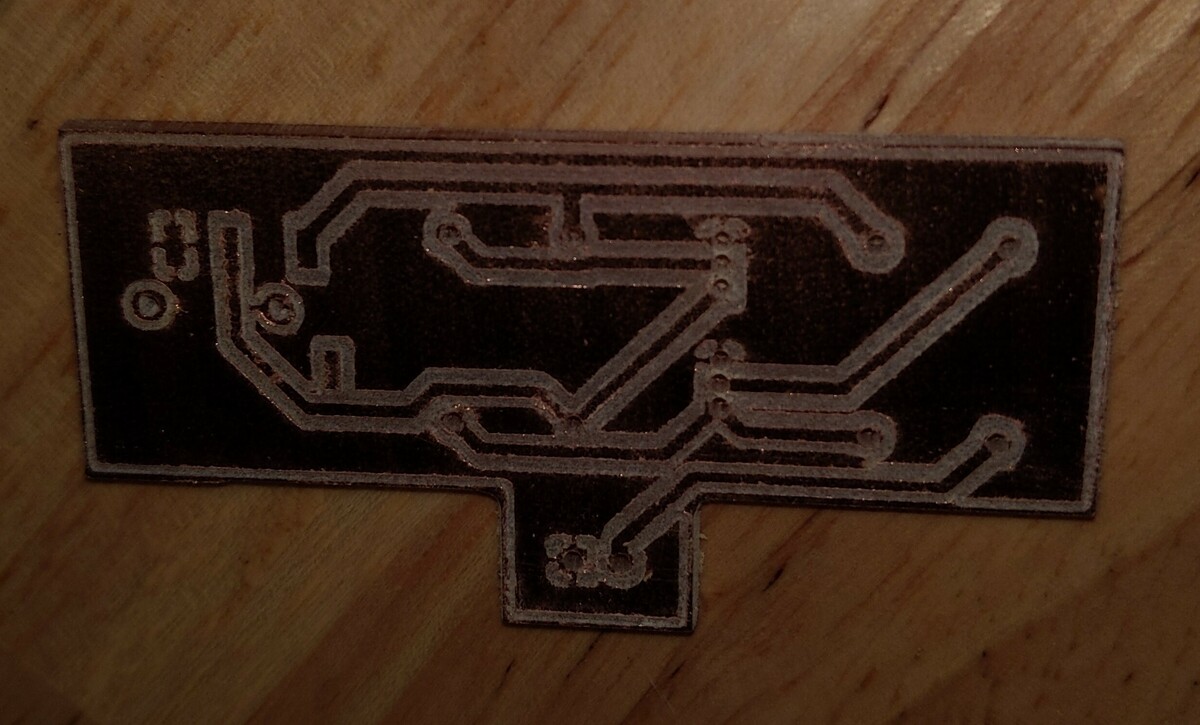
Overall, I was happy with the final result, though soldering was more challenging without a solder mask. As a quick reminder about cutting female pin headers, pull out the pin on the slot you want to cut on and score the header so that it’s easier to break.

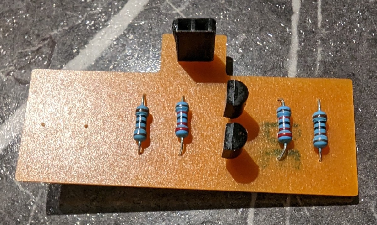
Two things I would like to improve on later would be milling with something that didn’t burr the copper up on the sides of the track cuts, and look into solder masks for easier soldering.